May 1, 2026
Harvard Team Claims Record Efficiency In Chip-Scale UV Light
A new fabrication method delivers 120 times more on-chip UV power than previous designs.
For decades, getting meaningful ultraviolet light out of a chip-scale device has been one of photonics research's most stubborn technical challenges. The physics were promising. The fabrication reality was not. A new study out of Harvard may have finally changed that calculus.
Researchers in the lab of Marko Lončar at Harvard's School of Engineering published findings on April 21 in Nature Communications showing a chip-scale UV light source that produces roughly 120 times more output power than previous comparable designs. The device generates 4.2 milliwatts of on-chip UV power at 390 nanometers, a threshold the researchers describe as the first time this platform has crossed into practical relevance.

What They Actually Built
The device works by converting red light into UV light on-chip, a process called frequency upconversion, using a crystalline material called thin-film lithium niobate. The material is already well-regarded in photonics for its efficiency at infrared wavelengths. What the Harvard team demonstrated is that it works for UV generation, too, provided you solve the fabrication problems that have blocked progress until now.
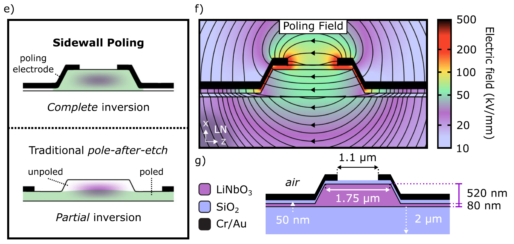
Image Credit: Nature.com "Milliwatt-level UV generation using sidewall poled lithium niobate"
The key invention is a technique called sidewall poling. Without getting lost in the physics, the method places electrodes directly against the sides of microscopic light-guiding channels etched into the chip, rather than above or below them. That placement allows the crystal structure to be precisely and uniformly reconfigured, which is what makes efficient light conversion possible. Earlier approaches left too much of the waveguide improperly treated, bleeding efficiency the whole way.
As co-first author Kees Franken put it: "When people think about lithium niobate, they don't think of it as a UV material, but we show that it is."
Why This Might Be Worth Watching
This is not a UV-C disinfection story, and it would be a mistake to read it that way. The wavelength demonstrated here, 390 nanometers, sits at the near-UV edge, closer to violet than to the germicidal UV-C range. It will not replace the LED modules currently used in air and surface disinfection systems.
What it does point toward is a longer-term shift in how UV light gets packaged and deployed. The researchers note potential applications in compact environmental sensors for greenhouse gas monitoring, quantum computing hardware, and precision optical instrumentation. These are specialty markets, not core commercial lighting. But they are markets where integrated photonics and lighting technology increasingly overlap, and where form factor constraints are exactly the kind of problem this work addresses.
For lighting people tracking where photonics and illumination are converging, the more useful question is not what this chip does today. It is what becomes possible when UV generation stops being the constraint.